Abstract
This article provides a detailed explanation of considerations for mixed-signal PCB layout design. It covers aspects of component placement, circuit board layout, and grounding plane considerations. The guidelines discussed in this article offer a practical approach to layout design for mixed-signal boards and should be helpful to engineers of all backgrounds.
Introduction
Mixed-signal PCB design demands a fundamental understanding of both analog and digital circuits to minimize, if not prevent, signal interference. The components that make up modern systems operate in both the digital and analog domains, and they must be carefully designed to ensure signal integrity across the entire system.
As a critical part of the mixed-signal development process, PCB layout can be daunting, and component placement is just the beginning. There are other factors to consider, including the various layers of the circuit board and how to manage them properly to minimize interference caused by parasitic capacitance (which can unintentionally occur between layers of the PCB).
Grounding is also a crucial step in PCB layout design for mixed-signal systems. While grounding is a topic often debated in the industry, it's not necessarily the simplest task for engineers to standardize a method. For instance, a single issue with high-quality grounding can impact the entire layout of a high-performance mixed-signal PCB design. Therefore, this aspect should not be overlooked.
Component Placement
It's similar to building a house, a system's floor plan must be created before placing circuit components. This step establishes the overall integrity of the system design and should help avoid high-noise signal interference.
When creating the floor plan, it's recommended to follow the signal paths from the schematic, especially for high-speed circuits. Component placement is also a critical aspect of the design. Designers should be able to identify critical functional blocks, signals, and connections between blocks to determine the optimal placement of components within the system. For example, connectors are best placed at the edge of the board, while auxiliary components like decoupling capacitors and crystals should be positioned as close as possible to the mixed-signal devices.
Separation of Analog and Digital Modules
To minimize the common return path for analog and digital signals, it is advisable to consider separating analog and digital modules so that analog signals do not mix with digital signals.
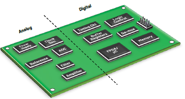
► Sensitive analog components, such as amplifiers and voltage references, should be placed within the analog plane. Similarly, high-noise digital components, like logic control and timing modules, must be placed on the other side/digital plane.
► If the system includes a mixed-signal analog-to-digital converter (ADC) or digital-to-analog converter (DAC) with low digital current, the approach for this can be similar to that of analog components within the analog plane.
► For designs with multiple high-current ADCs and DACs, it is recommended to separate analog and digital power supplies. In other words, AVCC should be tied to the analog portion, while DVDD should be connected to the digital portion.
► Microprocessors and microcontrollers may occupy space and generate heat. These devices should be placed at the center of the circuit board for better heat dissipation, while also being positioned close to the associated circuit modules.
Power Modules
The power supply is a crucial part of any circuit and should be handled carefully. It is generally recommended that power modules be isolated from the rest of the circuit while still being located close to the components they supply power to.
In more complex systems where devices may have multiple power pins, separate dedicated power modules can be used for the analog and digital sections to avoid high-noise digital interference.
On the other hand, power routing should be kept short and direct, with wide traces to reduce inductance and prevent current limitations.
Decoupling Techniques
Power Supply Rejection Ratio (PSRR) is one of the critical parameters designers must consider in achieving the desired system performance. PSRR measures a device's sensitivity to variations in the power supply, ultimately determining the device's performance.
To maintain optimal PSRR, it is essential to prevent high-frequency energy from entering the device. This can be achieved by appropriately decoupling the device's power supply to a low-impedance ground plane using a combination of electrolytic and ceramic capacitors.
The purpose of proper decoupling is to create a low-noise environment for circuit operation. The fundamental rule is to provide the easiest path for the current to return by offering the shortest paths.
Designers should pay attention to high-frequency filtering recommendations for each device. More importantly, this list serves as a guideline, providing general decoupling techniques and their correct implementation methods.
1.Electrolytic capacitors serve as charge storage devices for transient currents, reducing low-frequency noise on the power supply, while low-inductance ceramic capacitors are used to reduce high-frequency noise. Additionally, ferrite beads are optional but provide increased high-frequency noise isolation and decoupling.
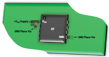
2.Decoupling capacitors should be placed as close to the power pins of devices as possible. These capacitors should be connected to a larger area of the low-impedance ground plane through vias or short traces to minimize additional series inductance.
3.Smaller capacitors (typically 0.01μF to 0.1μF) should be placed as close as possible to the power pins of devices. This arrangement prevents instability when devices have multiple output switches. Electrolytic capacitors (typically 10μF to 100μF) should not be more than 1 inch away from the power pins of devices.
4.For easier implementation, it is possible to connect decoupling capacitors to the ground plane near the device's GND pins through vias in a T-shaped configuration rather than creating traces.
See the example in Figure 2.
Circuit Board Layers
Once component placement and the board layout plan are completed, we can look at another aspect of circuit board design, often referred to as board layers. It is highly recommended to consider the board layers before PCB routing, as this will determine the allowed return paths for the system design.
Board layers refer to the vertical arrangement of copper layers within the circuit board. These layers should manage the current and signals throughout the entire circuit board.

Typically, high-performance data acquisition systems should have four or more layers. The top layer is usually used for digital/analog signals, while the bottom layer is used for ground signals. The second layer (ground plane) serves as a reference plane for impedance-controlled signals, reducing IR voltage drops and shielding digital signals on the top layer. Finally, the power plane is located on the third layer.
Power and ground planes should be adjacent to each other, as they provide additional interplane capacitance, aiding in high-frequency decoupling for the power supply.
Regarding the ground plane, recommendations for hybrid signal designs have evolved over the years. For years, it made sense to split the ground plane into analog and digital sections. However, for modern mixed-signal devices, a new approach is recommended. Proper plane planning and signal separation should help prevent issues related to high-noise signals.
Ground Plane: Separate or Not?
Grounding is an important step in mixed-signal PCB layout design. A typical 4-layer PCB must have at least one layer dedicated to a ground plane to ensure that return signals have a low-impedance path back. All integrated circuit ground pins should be routed and directly connected to the low-impedance ground plane, minimizing series inductance and resistance.
For mixed-signal systems, separating analog and digital grounds has become a standard grounding practice. However, it is best to manage mixed-signal devices with low digital currents through a single ground. Furthermore, designers must consider which grounding approach is most suitable based on mixed-signal current requirements. Designers must weigh the pros and cons of these two grounding approaches.
Single Ground Plane
For mixed-signal systems with a single low digital current ADC or DAC, a single solid ground plane can be the best approach. To understand the importance of a single ground plane, we need to revisit return currents. Return currents refer to the currents that return to the ground and form a complete loop between devices through the traces on the PCB to prevent mixed-signal interference.
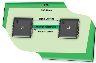
Figure 4. Return Currents in a System with a Single Solid Ground Plane
The simple circuit shown in Figure 4 illustrates the advantages of a single solid ground plane over separate ground planes. Signal currents have equal but opposite return currents. These return currents flow back to the source through the ground plane, following the path with the lowest impedance.
For low-frequency signals, return currents follow the path with the least resistance, which is often a straight line between the ground reference points of the devices. However, for higher-frequency signals, a portion of the return current will try to follow the signal path. This is because the impedance along this path is lower, forming the smallest loop between outgoing and returning currents.
Separation of Analog and Digital Grounds
For complex systems where implementing a single solid ground approach is challenging, separating the ground is more suitable. Separate ground planes are another common method, where the ground plane is divided into two: an analog ground plane and a digital ground plane. This is appropriate for more complex systems with multiple mixed-signal devices and high digital current consumption.

Figure 5 shows an example of a system with separate ground planes.
For systems using separate ground planes
the simplest solution for achieving an overall ground is to eliminate interruptions in the ground planes and allow return currents to take a more direct path back through a star grounding point. A star grounding point is the junction where analog and digital ground planes are connected in mixed-signal layout designs.
In typical systems, star grounding can be associated with a simple narrow continuous junction between analog and digital ground planes. For more complex designs, star grounding is usually achieved by jumpering to grounding pads. No current flows through the star ground, so no heavy current-carrying pads and jumper shunts are needed. The main purpose of star grounding is to ensure that both grounds share the same reference level.
Designers should ensure that they check the grounding recommendations provided in the datasheets of every device to ensure compliance with grounding requirements and to avoid grounding-related issues. On the other hand, mixed-signal devices with AGND and DGND pins can connect to their respective ground planes because star grounding also connects both grounds at one point. This way, all high-noise digital currents flow through the digital power and ground planes, staying isolated from the sensitive analog circuits. The isolation of AGND and DGND planes must be achieved on all layers of the multilayer PCB.
Other Common Grounding Practices
You can follow these steps or checklists to ensure that the appropriate grounding scheme is implemented in mixed-signal/digital systems:
Connections at star grounding points should be made using wider copper traces.
Check for narrow traces on the ground plane, as these connections are unnecessary.
Provide pads and vias to facilitate the connection of analog and digital ground planes when necessary.
Conclusion
PCB layout for mixed-signal applications can be quite challenging. Creating a component placement plan is just the starting point. When striving to achieve the best performance for mixed-signal system layouts, managing the PCB layers correctly and developing suitable grounding schemes are critical aspects that system designers must consider. Establishing a component placement plan will help lay the foundation for the overall integrity of the system design. Organizing the PCB layers appropriately will aid in managing the current and signals across the entire circuit board. Finally, choosing the most favorable grounding scheme will enhance system performance and prevent issues related to high-noise signals and return currents.
混合信号PCB布局设计的基本准则 - 模拟/电源 - -EETOP-创芯网