


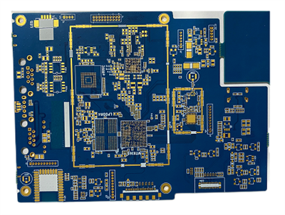
HDI Circuit Board
BS Interconn Hong Kong Co., LIMITED established in January 2019, which focusing on the global business of HIGH FREQUENCY, HIGH SPEED, HIGH CONDUCTIVITY printed wiring boards. The company's main products include multilayer PCBs, HDI circuit board, conventional rigid PCB, rigid-flex PCB, special PCB and so on.
HDI Printed Circuit Boards
BS Interconn Hong Kong Co., Limited is a source of HDI printed circuit boards for small size high performance electronics. We specialises in printed wiring boards for high frequency, high speed and high conductivity applications, including HDI circuit boards, which are included in its multilayer PCB family.
Why HDI Boards Work Well
The smaller boards that are possible using HDI technology without compromising performance. Microvias provide more reliability than conventional through-hole vias, and via-in-pad and blind-via techniques reduce the signal delays and increase the signal integrity. This is important in products where a clean signal flow and tight spacing are both important.
Other practical benefits include:
Better reliability through microvia use
Stronger signal quality with fewer stubs
A more compact board layout
Lower overall cost potential through smarter layer use
Key Specs from BSI
According to BSI's listed board details, it is a 6-layer controlled impedance board with an ENIG surface finish. The material option is low-loss / low-Dk, high-performance FR-4 (EM-528K), with the minimum track and gap being 0.508 mm, 2.0-ounce finished copper. Post bonded core thickness is 1.2mm.
These specs are appropriate for designs that require consistent routing, small spacing, and predictable signal performance.
HDI Circuit Board Types
BSI highlights four common HDI board types:
- Improved reliability by using microvia.
- Better signal propagation with fewer stubs.
- A smaller layout of the board
Improve overall cost potential by intelligent use of layers
Service, Packaging, and Ordering
BSI has established itself as a customer-centric supplier with a one-stop solution and over 10 years of experience in the industry. Sealed bags, anti-static bags, foam bags for PCBA and customised carton labelling are available.
We is able to accept the terms of delivery that include FOB, CFR, CIF, EXW, FCA, DDP, DDU, and express delivery, and it is able to accept USD, EUR, HKD, GBP, and CNY currency. Payment terms are available in T/T, L/C, D/P, D/A, MoneyGram, PayPal and Western Union.
-
![HDI PCB Manufacturer in China | High Density Interconnect PCB Supplier]()
HDI PCB Manufacturer in China | High Density Interconnect...
HDI boards are commonly used in products that require compact layouts, including smartphones, laptops, wearable devices, communication equipment, automotive radar systems, and medical electronics.AsAdd to Inquiry -
![High-speed Circuit Board]()
High-speed Circuit Board
It needs impedance matching for some types of signals which are about 40-120 ohms. And characteristic impedance matched hints are antennae and many differential pairs.It's important for designer toAdd to Inquiry -
![E-cigarettes Boards]()
E-cigarettes Boards
E-cigarettes boards refer to the printed circuit boards (PCBs) used in electronic cigarettes or vaping devices. These boards play a crucial role in regulating various functions of the e-cigarette,Add to Inquiry -
![IoT Circuit Boards]()
IoT Circuit Boards
IoT circuit boards are typically designed to be compact, energy-efficient, and capable of wireless communication to enable seamless connectivity between devices. They can be found in a wide range ofAdd to Inquiry -
![RoHS Compliant PCB]()
RoHS Compliant PCB
RoHS (Restriction of Hazardous Substances) compliant PCB refers to a printed circuit board that meets the requirements and restrictions set forth by the RoHS directive. The RoHS directive restrictsAdd to Inquiry -
![High-Density Interconnect PCB]()
High-Density Interconnect PCB
In the process of multi-core laminate production, the alignment of inner core plates directly affects the quality of products. For the inner core plate before lamination, the AB surface has theAdd to Inquiry -
![High TG PCB Materials]()
High TG PCB Materials
What is TG in PCB material? Temperature profiles for PCB material are typically given in terms of the material's Tg (Glass Transition Temperature). This measure records the temperature at which theAdd to Inquiry -
![High Density Circuit PCB]()
High Density Circuit PCB
High density PCB means a compact circuit board, which is to increase component interconnect density, it is necessary to compress the circuit and interconnection space from a geometric perspective,Add to Inquiry -
![Optical Module PCB]()
Optical Module PCB
The reception part takes an optical signal with a specific bit rate as input, which is converted into an electrical signal by an optical detector diode within the module. It then outputs anAdd to Inquiry -
![High-speed Circuit Board]()
High-speed Circuit Board
High-speed circuit boards are a specialized type of circuit board that can handle billions of operations within a single second. These PCBs employ multiple microprocessors and other powerfulAdd to Inquiry


Why choose us?
High quality
We aim to be the most preferred supplier of our partners by providing high quality products at suitable cost leveling in different fields.
Rich experience
We have a professional technical team with more than 10 plus years of experience in the PCB industry which adhere to commit to provide professional advisement, continuous and satisfactory PCB services to all our customers around the world.
One-stop solution
To enhance customer satisfaction, we go beyond the conventional by offering comprehensivevalue-added services as a one-stop solution.

Improved reliability
Due to their smaller aspect ratio, microvias offer better reliability compared to typical through-hole vias. They are more robust than through-holes and employ superior materials and components, resulting in excellent performance for HDI (High-Density Interconnect) technology.
Enhanced signal integrity
HDI technology incorporates via-in-pad and blind-via techniques. These techniques help bring components closer to each other, reducing the length of signal paths. HDI technology eliminates stubs caused by through-holes, reducing signal reflection and improving signal quality. Therefore, shorter signal paths significantly enhance signal integrity.
Cost-effectiveness
With proper planning, HDI technology can reduce overall costs compared to standard PCBs. This is due to the requirement of fewer layers, smaller dimensions, and fewer PCBs needed.
Compact design
The combination of blind and buried vias reduces the space requirements of the circuit board.
|
BSI´s PCB Features |
BSI´s technical spec |
|
Number of layers |
6 layers |
|
Technology highlights |
Controlled impedance,ENIG |
|
Materials |
Low loss / low Dk, higher performance FR-4(EM-528K) |
|
Dielectric thickness |
0.508mm |
|
Copper weights (finished) |
2.0 ounce |
|
Minimum track and gaps |
0.12mm / 0.12mm |
|
Core thickness |
1.2mm post bonded |
|
Surface finishes available |
ENIG |
Types of HDI Circuit Board

Standard HDI PCBs
Standard high density interconnect PCBs utilize a combination of micro, blind and buried vias to build a high-density interconnection structure. These are a common type among HDI printed circuit boards and they are commonly used in communication devices and consumer electronics. Standard HDI PCB boards will have a multi-layer stack-up which will allow the PCB for complex routing and signal transmission at a high speed rate.

Build-up HDI PCBs
Build-up high density interconnect PCBs are categorized by their sequential lamination process which includes adding additional layers to the board one at a time. This sequential lamination process provides good flexibility in circuit design and layer count. They are highly applicable in areas where space is so limited but performance needs to be the best such as in smartphones and tablets.

Laser drilled HDI PCBs
These printed circuit boards utilize laser drilling technology to form micro vias in precise regions and areas. Laser drilling technology will provide very fine holes and it will have better control over via placement. In specific HDI PCB fabrication, Laser-drilled HDI printed circuit boards are ideal for high-speed and high-frequency applications due to the accuracy of the vias formed.

Embedded component HDI PCBs
Embedded component HDI PCB boards are HDI printed circuit boards within the layers of the PCB itself. This will reduce the overall size of the device and improve the performance of it. They are pretty useful in applications where space is extremely limited and component density is critical.
PCB: Sealed bag, Anti-static bags, Suitable carton.
PCBA: Antistatic foam bags, Anti-static bags, Suitable carton.
Customized packaging: The carton outside will be printed the name of the customer address, mark, the customer needs to specify the destination and other information.


Shipping

Payment Methods
Accepted Delivery Terms
FOB, CFR, CIF, EXW, FCA, DDP, DDU, Express Delivery;
Accepted Payment Currency
USD, EUR, HKD, GBP, CNY;
Accepted Payment Type
T/T, L/C, D/P D/A, MoneyGram, PayPal, Western Union.
Certifications


FAQ
As one of the leading hdi circuit board manufacturers and suppliers in China, we warmly welcome you to buy cheap hdi circuit board for sale here from our factory. All customized products are with high quality and low price.
Multilayer PCBs, , HDI Circuit Board