
Multilayer PCBs
Full Service, China Multilayer PCBs Designer and Manufacturer
Focus on R&D
Our company has a professional technical team with more than 10 years of experience in the PCB industry.
Quality Assurance
We use high-quality raw materials and advanced processing equipment to produce all PCBs, and have designed strict production standards and testing procedures.
Rich experience
Our rf circuit boards have been sold all over the world, so we have rich experience and knowledge to answer all your questions about design and manufacturing.
After-sales service
We have set up a dedicated customer service team to provide customer service 24 hours a day, so your after-sales problems can be responded to quickly.
-
![Why Engineers Choose Rogers 4003C Instead Of Standard FR4]()
Why Engineers Choose Rogers 4003C Instead Of Standard FR4
The global expansion of 5G, autonomous driving, AI networking infrastructure, and IoT devices continues increasing demand for high-frequency materials.As signal speeds continue increasing, materialAdd to Inquiry -
![HDI PCB Manufacturer in China | High Density Interconnect PCB Supplier]()
HDI PCB Manufacturer in China | High Density Interconnect...
HDI boards are commonly used in products that require compact layouts, including smartphones, laptops, wearable devices, communication equipment, automotive radar systems, and medical electronics.AsAdd to Inquiry -
![Two Depth Cavity P Circuit Board(POP Board)]()
Two Depth Cavity P Circuit Board(POP Board)
At BS Interconn, we deliver innovation through our Two-Depth Cavity Printed Circuit Boards , engineered specifically for Package-on-Package (PoP board) applications. This advanced PCB solutionAdd to Inquiry -
![IoT 10 Layers PCB]()
IoT 10 Layers PCB
In today's fast-paced office environments, the demand for high-performance electronics has skyrocketed. Among the innovations driving this change is the IoT 10 layers PCB-a versatile and powerfulAdd to Inquiry -
![HDI Rigid-Flex Board-26L]()
HDI Rigid-Flex Board-26L
With the rapid growth of the HDI Rigid-Flex Board market, the industry is progressively advancing toward high reliability, higher layer counts, and HDI trends. Customers of high-layer HDI Rigid-FlexAdd to Inquiry -
![Set-top Box PCB]()
Set-top Box PCB
This type of foldable circuit is known as a flexible circuit, flexible PCB, or FPC. It is typically composed of polyimide or polyester film with a polymer coating that protects the conductive circuitAdd to Inquiry -
![High-speed Circuit Board]()
High-speed Circuit Board
It needs impedance matching for some types of signals which are about 40-120 ohms. And characteristic impedance matched hints are antennae and many differential pairs.It's important for designer toAdd to Inquiry -
![Halogen Free Boards]()
Halogen Free Boards
Modern vehicles rely heavily on electronics. Halogen-free pcbs are used in automotive control units, sensors, infotainment systems, and engine management, ensuring safety and reduced environmentalAdd to Inquiry -
![Flexible Wiring Board]()
Flexible Wiring Board
A flexible wiring board, also known as a flex PCB or flexible printed circuit board, is a type of electronic circuit board that is designed to be flexible and bendable. Unlike rigid PCBs, which areAdd to Inquiry -
![Rigid Single Board]()
Rigid Single Board
Extreme Conditions and High Temperatures Are Typical in This Business. Stiff Pcbs Can Be Useful in This Situation Since They Can Get Made Using Large-Temperature Laminations and Aluminum or CopperAdd to Inquiry -
![Half Hole On Module PCB]()
Half Hole On Module PCB
In the PCB industry, half-holes, also known as stamp holes, are primarily used to make connections solder. Half-holes are typically created on the PCB's very edge, with a second hole being milledAdd to Inquiry

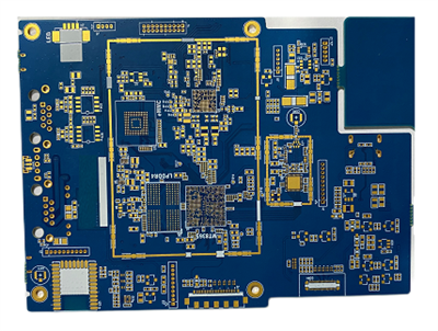


What is a Multilayer PCB?
Multilayer PCB refers to a multi-layer printed circuit board made of epoxy resin-infused fiberglass boards and a conductive core material laminated. It adds an intermediate conductive copper layer on the basis of a double-sided printed circuit board, with a layer structure of at least 4layers and up to 100 layers.
These copper layers are connected through various methods such as plated through holes, through holes and buried holes, which can provide more circuit routing space for complex applications. They enable multi-layer PCBs to have high signal transmission capabilities in a small form factor and eliminate external EMI interference and crosstalk issues, and are widely used in electronic equipment, medical equipment, and wearable device applications.
Multilayer PCB Manufacturing Process
Pre-production: Generate PCB-specific manufacturing data based on customer-provided data and determine process steps and related inspections. At the same time, cut the substrate to the desired size.
Inner layer:
- Use photosensitive film to transfer the circuit image to the board surface
- Use etching to remove unwanted copper from the panel, leaving the target circuit behind
- Verify that the circuit matches the design and has no defects
- "Stack" with insulating prepreg and add to the top and bottom of the stack.
Drilling: Plated drilling (PTH) is accomplished by laser drilling, and PTH is followed by panel plating, providing a thicker copper deposit of 5 to 8 microns.
Outer layer:
- Use photosensitive dry film for image transfer (similar to the inner layer process) and expose it to UV light and etching, then remove the dry film.
- Add additional plating layer in the area without dry film, and the average through hole is 25um/min 20um.
- Etch the exposed copper to chemically remove tin deposits from the circuit.
- Scan the imaged and etched panel to ensure there are no defects in the circuitry.
Surface treatment:
- Prepare the solder mask ink or epoxy resin and the prepared template, and use the screen printing process to push the ink or resin into the holes.
- Apply solder mask ink to the entire PCB surface, exposing part of it to UV light to completely cure. Other parts are removed and used as weldable surface parts.
- Through various surface treatments, including electroless nickel plating, immersion gold, spray tin, immersion silver, etc.
Cut: Fabricated panels are cut to specific sizes and shapes. Prepare for assembly by scoring, routing, or drilling holes.
Quality Inspection:
- Use probes and clamps to inspect trace and through-hole interconnect details to ensure there are no opens or shorts on the finished board.
- According to the acceptance criteria, the inspector conducts visual and manual inspection of the PCB, including size, solderability, etc.
Multilayer PCB Materials and Construction
Conductive Layers
The conductive layers of multilayer PCBs are made from conductive materials, including rolled copper foil or electrolytic copper with metal finishes and 1⁄2 to 3 oz thickness. Its main function is to connect different components so that data or power signals can be transmitted between them.


Dielectric layer
The dielectric layer is made of insulating materials such as FR-4 fiberglass reinforced epoxy, PTFE (Teflon), polyimide, and cyanate ester. These insulating materials can isolate circuits between conductive layers and prevent circuit short circuits and failures caused by leakage.
Adhesive layer
The adhesive layer is used to glue each layer of the multi-layer PCB together. Its common materials are FR-4 prepreg and fluoropolymer adhesive film, which make the layers stronger, insulate and prevent leakage.

What Are The Applications Of Multi-Layer PCBs?

Medical equipment
With the same signal transmission capability, multi-layer PCBs are small in size and light in weight, and can be easily integrated into medical equipment, including in vitro diagnostic instruments, MRI, CT detectors, etc.
Household appliances
Multi-layer PCB can shorten the signal path, reduce loss and delay in the signal path, and improve the response speed of smart TVs, music players and other devices.
Computer equipment
Multi-layer PCB can reduce the size and power consumption of the circuit board. It is used in graphics cards, motherboards, computer mice and other products, and can reduce noise during work.
Telecom Electronics
Multilayer PCB is used for GPS and satellite applications and signal transmission. Various signal lines and power lines can be arranged on different layers in it to reduce signal interference and crosstalk.
Aerospace
The aviation industry has high requirements on the weight, volume and temperature of PCBs, and the fr4 material used in multi-layer PCBs can withstand high temperatures and pressures, making it used in aircraft navigation, communications, radar and other equipment.
Multi Layer PCB Boards – Technical specification
| Feature | Technical specification |
| Number of layers | 4 – 22 layers standard, 30 layers advanced, 40 layers prototype. |
| Technology highlights | Multiple layers of epoxy glass fiber bonded together with multiple layers of copper of varying thicknesses. |
| Materials | High performance FR4, halogen-free FR4, low loss and low Dk materials |
| PCB thickness | 0.40mm – 7.0mm |
| Minimum laser drill | 0.10mm standard, 0.075mm advanced |
| Minimum mechanical drill | 0.20mm |
| Copper weights(finished) | 18μm – 210μm, advanced 1050μm / 30oz |
| Minimum track and gaps | 0.075mm/0.075mm |
| Metal core thickness | 0.4-2mm post bonded |
| Macimum dimensions | 580mm x 1080mm, advanced 610mm x 1400mm |
| Surface finishes avaiable | HASL (SnPb), LF HASL (SNiCu), OSP, ENIG, Immersion Tin, Immersion Silver, Electrolytic gold, Gold fingers |
What Are The Advantages Of Multilayer Printed Circuit Board?

Stable operation: Multilayer PCB uses FR-4 material as its base material, epoxy resin and polyimide as the solder mask layer, and copper foil and aluminum foil as the conductive material. These materials ensure tight connections between PCB layers and stable electrical transmission capabilities, which prevent short circuits and poor contact.
Durable: Multilayer PCBs have a larger number of layers and thicknesses, and use heat and pressure to bond the individual conductive layers together through lamination. Due to the mutual support between its internal layers, the structure of the PCB is more stable and less prone to deformation or fragmentation due to impact.
High conductivity: The conductive layer of the multi-layer PCB uses an immersion gold surface treatment process to cover the surface with a uniform and dense metal layer. The thickness of the immersed gold layer is generally 0.05-0.15um, and it only contains nickel and gold, which is tightly combined with the copper layer and is not prone to short circuit when transmitting signals.

Flexible connection: Multilayer PCB can realize the design of short-range, long-range, and ring lines through conductive connections between layers. Users can also use different types of vias, blind holes, intra-board copper foil segmentation and other processing methods to make their layout more flexible in different applications.
High sealing: Multilayer PCB uses SMT chip technology, and the components and PCB substrate are welded together through wave soldering or reflow soldering. The packaging density of each component inside is very high, which protects the internal wires and connectors from short circuits and poor contacts.
Environmental friendly: Multi-layer PCB uses ROHS certified base materials and welding materials, and can be recycled after being discarded. Moreover, it adopts scientific environmental control measures during the production process to effectively reduce energy consumption and carbon dioxide emissions.
Our Certificate


Know More About Multilayer PCBs
Q: How do multi layer PCBs work?
Q: What is the difference between single and multilayer PCB?
Q: How many layers can a PCB be?
Q: What are the small holes in printed circuit boards called?
Q: What is the difference of a 4 layer PCB over a 2 layer PCB?
Q: How do you stack 4 layer PCB?
- Includes 3 signal layers and 1 GND (ground) layer.
- Includes 2 signal layers, 1 GND (ground) layer and 1 VCC (power supply) layer.
Q: How do I choose a layer for PCB?
- Circuit complexity: The number of components and connections required for the circuit will determine the number of layers required. Complex circuits will require more conductive layers.
- Cost: The manufacturing costs of single-layer and double-layer PCBs and multi-layer PCBs are different. Each additional layer of conductive copper increases the manufacturing cost of the PCB.
- Signal Integrity: Analyze the signals traveling in the circuit and select the layers that provide the ideal balance between signal integrity and cost.
- Frequency of use: For higher speeds and operating capabilities, multi-layer PCB is essential, providing you with high signal transmission capabilities.
Q: What is the most important layer in a printed circuit board?
Q: Why copper layer is used in PCB?
- Because copper is a common thermal and electrical conductor, it can improve heat transfer between PCBs and reduce destructive stress caused by uneven heating.
- Compared to other metals, copper has a low resistance and can transmit electricity quickly and efficiently.
- Copper is flexible and can be easily molded into different shapes and sizes, forming a strong bond with other metals.
Q: What is ground guarding in PCB?
Q: What is the name of technology used to mount components on multilayer PCBs?
- Surface Mount Technology (SMT): Components are mounted or placed directly on the surface of a printed circuit board (PCB).
- Through-Hole Mount (THM) Technology: The assembler places component leads into holes drilled in the exposed PCB.
Q: What is FR4 made of?
Q: What is the difference between G10 and FR4?
- Material Composition: G10 is made purely of epoxy resin and woven fiberglass cloth while FR4 is a composite material made of a combination of fiberglass cloth and epoxy resin with a flame retardant additive.
- Electrical Properties: FR4 has flame retardant additives component, and its operating temperature range is higher than G10, without losing its physical properties.
Q: What are the main benefits of using multilayer PCBs?
- Small size: Multi-layer PCB uses a layered design to reduce the size by increasing the number of layers to provide very high signal transmission effects.
- Light weight: Because its panel size becomes smaller, so does its component size, making it ideal for small precision devices such as wearable smart watches.
- Durable: Its multi-layer construction allows it to be thicker and can withstand harsher conditions as well as impacts.
- Simplicity: It allows high-density components to be easily deployed on its surface, which not only facilitates wiring but also makes circuit board connections closer.
Q: What design challenges are unique to multilayer PCBs?
- Component Placement: Components must be arranged in such a way that they don't interfere with each other while being placed in the smallest area possible.
- Signal Integrity: Signal integrity issues such as noise, crosstalk, signal distortion, and signal loss can lead to serious problems.
- Thermal Management: The temperature of the board must not exceed safe limits, which can cause malfunctioning of the PCB.
- EMC and EMI: Electromagnetic Compatibility (EMC) and Electromagnetic Interference (EMI) must be taken into account when designing PCBs.
Q: What types of testing are used to ensure multilayer PCB quality?
- Appearance test: The operator checks the PCB surface for scratches, welding or joint problems, etc.
- Automated Optical Inspection (AOI): This system captures images of circuits and provides defects, if any, as output to engineers for repair based on comparison and available data related to the design.
- X-ray inspection: X-rays can be absorbed by heavy metals such as lead used in PCBs to obtain internal views of solder joints and connections.
- Probe inspection: We use electronic probes to check the positioning and assembly of each component installed on the PCB, checking its capacitance, resistance and other parameters.
- Functional test: Engineers check the PCB’s soldering position, signal transmission and EMI shielding capabilities, and whether it meets all set standards.
Q: Why is the number of layers in a multilayer PCB even?
Q: What are the grounding methods for multilayer PCBs?
- Ground wiring All grounded components are connected via a common trace.
- Public ground plane Free space on the PCB not utilized by traces or components is covered with ground to improve thermal characteristics and reduce electromagnetic interference (EMI).
- Ground via Components are connected to the ground plane through ground vias.
- Power system grounding All ground connections are connected to a ground busbar, which is connected to a ground conductor, which is connected to a ground rod or ground grid, collecting all ground wires from all installations to a common point.
- Equipotential grounding By electrically connecting equipment chassis, metal pipes and other grounding devices, each conductive element should have the same ground potential.
Q: What is the standard thickness of PCB?
Q: How much does it cost to make a multilayer PCB?
As one of the leading multilayer PCBs manufacturers and suppliers in China, we warmly welcome you to buy cheap multilayer PCBs for sale here from our factory. All customized products are with high quality and low price.
Buried PCBs Backplane